MICROPROCESSORS- OVERVIEW
Content
- INTRODUCTION
- ORIGIN AND EVOLUTION OF MICROPROCESSORS
- EXPLANATION OF BASIC TERMS
- HOW DOES MICROPROCESSOR WORK?
- MICROPROCESSOR BASED SYSTEM
- CLASSIFICATION OF MICROPROCESSOR
- TYPES OF MEMORY
- APPLICATION OF MICROPROCESSOR
INTRODUCTION
The microprocessor is the heart of any computer system, it is an electronic chip that functions as a central processing unit (CPU) of a computer, providing computational control.
Microprocessor based systems with limited resources are called microcomputers.
Block diagram of basic microcomputer:
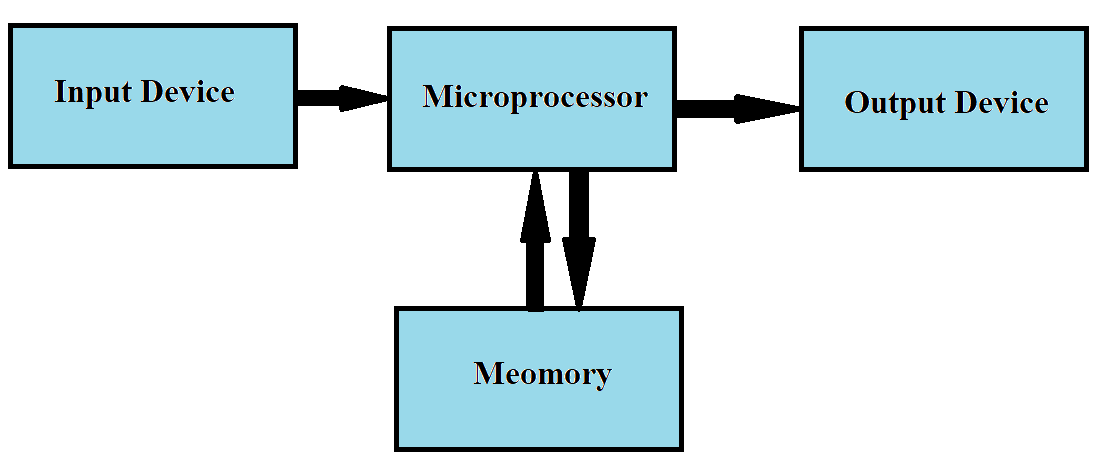
A basic microprocessor chip has arithmetic and logic functional units along with the associated control logic to process the instruction execution. Programs or instructions to be executed by the microprocessor are stored sequentially in memory locations. The microprocessor fetches the instructions sequentially and executes them in its arithmetic and logic unit (ALU). So all microprocessors have a built-in memory access, management part and some amount of memory.
Manufacturers of any microprocessor give its list of instructions in two forms:
- Mnemonic
- Binary machine code
Mnemonic:
It is easy to understand and usually programs are written through it. It is assembly level language.
Binary machine code
Through this code microprocessors work and it is difficult to understand.
ORIGIN AND EVOLUTION OF MICROPRCESSORS
Microprocessor was first invented in the 20th century. Invention of microprocessors was a great achievement in the industrial as well as technology field.
In the 1930s there was a mechanical calculating device for mechanical relays and till the 1950s it was replaced by vacuum tubes. The vacuum tubes were quickly replaced by transistors that led to the introduction of mini computers in the 1960s and personal computer revolution in the 1970s.
Transistors led to the development of complex devices called integrated circuits (ICs).
• Intel was the first micro processing unit (MPU).
EXPLANATION OF BASIC TERMS:
Chip:
A chip is a very tiny integrated circuit that has a specific circuit etched to it that performs a specific function.
Bit:
Bit is a single binary digit which is the fundamental storage unit of computer memory. A bit can have only two values that are 0 and 1.
Byte:
8 bit word is referred to as byte.
Nibble:
4 bit word is referred to as nibble.
Kilobyte:
1024 bytes is kilobyte.
Megabyte:
1024 kilobyte is megabyte.
Arithmetic and logic unit(ALU):
An arithmetic logic unit (ALU) is a combinational digital circuit that performs arithmetic and bitwise operations on integer binary numbers.
Microcontroller:
A microcontroller is a chip that includes microprocessor, memory, and input/output signal ports. Microcontrollers can be called as single-chip microcomputers.
Microcomputer:
The system formed by interfacing the microprocessor with the memory and I/O devices to execute the required programs is called microcomputer.
Bus:
A bus is a group of wires/lines that carry similar information.
System bus:
The system bus is a group of wires/lines used for communication between the microprocessor and peripherals.
Computer architecture:
The design, internal configuration, and accesses in a digital computer are together called computer architecture. It is a set of rules and methods that describe the functionality, organization, and implementation of computer systems.
Von-Neumann architecture:
The architecture in which the same memory is used for storing programs as well as data.
Harvard architecture:
The architecture in which programs and data are stored in two separate memory units.
Instruction Set:
It is the set of instructions that the microprocessor can understand.
Clock:
It is a circuit that generates the sequence of evenly spaced pulses that synchronise the activities.
HOW DOES MICROPROCESSOR WORK?
The basic function of the microprocessor is to fetch the instructions stored in the memory and execute those instructions sequentially that is one by one.
A microprocessor is programmed to perform any task that can be programmed by the user. To work with a microprocessor it is important to know all the features of the microprocessor by the user.
To work with real world data, programs are written by the user. With the help of input interfacing circuits and some electronic processing circuits (data converters and ports) these data are input to the microprocessor. After processing these data the output is given to output devices or circuits which again requires interfacing circuits and ports.
So a microprocessor-based system requires memory units and interfacing circuits for input and output.
These all together make a microcomputer system.
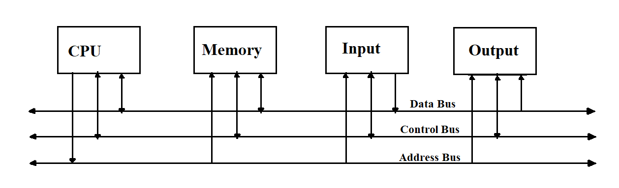
MICROPROCESSOR BASED SYSTEM
A system developed by a basic general-purpose microprocessor is called a microcomputer system. It consists of a CPU, memory unit and input/output ports.
microcomputer system requires three-bus architecture i.e. data bus, control bus, address bus.
Address bus:
The digital data sent by the processor is transported by the address bus. address bus consists of many lines for example an address bus of 8 bits corresponds to 8 lines of address and can address 2^8 different memory locations.
The addresses are written in hexadecimal number format.
Data bus:
The data bus transfers the data between the memory and processor or I/O device and the processor. An 8 bit processor generally has an 8 bit data bus.
Control bus:
For an appropriate data transfer between the processor and the peripherals, control bus is required. The control bus consists of signals for selection of the correct memory or I/O device from the address.
CLASSIFICATION OF MICROPROCESSOR
Microprocessor is classified on the basis of specification, application and architecture.
- Based on size of data:
4-bit, 8-bit, 16-bit, 32-bit and 64-bit microprocessor.
- Based on application:
(i) General-purpose processors: These types of processors are used in general computer integration.
E.g. Intel 8085
(ii) Microcontrollers: A microcontroller is a chip that includes microprocessor, memory, and input/output signal ports. Microcontrollers can be called as single-chip microcomputers.
(iii) Special-purpose processors: These types of processors are designed to perform special functions required for an application.
E.g. Digital signal processing.
- Based on architecture:
- RISC processors
- CISC processors
- VLIW processors
- Superscalar processors
TYPES OF MEMORY
Memory can be divided into four groups:
(i) Processor memory/register: These memory registers are few in number but they are fastest memory registers as these registers are within the processor. These memories are set of CPU registers.
(ii) Cache memory: In cache memory, those instructions are placed which are going to execute.It is the fastest external memory.
(iii) Primary or main memory: It is that storage area from where all programs are run.
Classification of primary memory:
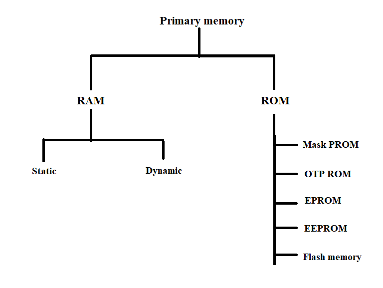
(iv) Secondary memory: These consist of slow devices like magnetic tapes and optical disks.
APPLICATION OF MICROPROCESSORS:
Microprocessor-based systems are thus found everywhere today.
(i) It is useful in the field of instrumentation: Frequency counters, function generators, frequency synthesizers etc.
(ii) It is used in communication equipment. These are used in digital telephone sets, telephone exchanges and modem etc. Teleconferencing possible due to use of microprocessors in television, satellite communication.
(iii) So Microprocessors are used in:
calculators,
games machine,
complex industrial controllers,
traffic light control,
multi user, multi-function environments,
military applications,
communication systems,
microwave oven, washing machine many more.
Questions
1. How many types of ROM are in primary memory?
(a.) 2
(b.) 3
(c.) 4
(d.) 5
Ans: (d.) 5. ROM is divided as Mask PROM, OTP ROM, EPROM, EEPROM, Flash memory.
2. Microprocessor consists of
(a.) Control unit
(b.) Registers
(c.) ALU
(d.) All of the above
Ans: d, All of the above
3. It is a group of wires/lines that carry similar information.
(a.) RAM
(b.) ROM
(c.) Bus
(d.) Chip
Ans: c, Bus
4.The architecture in which same memory is used for programs as well as data.
(a.) Harvard architecture
(b.) Von-Neumann architecture
(c.) Both
(d.) None
Ans: b, Von-Neumann architecture
5.Which is not the control bus signal?
(a.) WRITE
(b.) READ only
(c.) RESET
(d.) All the above
Ans: c, RESET
6.A microprocessor memory can be logically divided into?
(a.) 1
(b.) 2
(c.) 3
(d.) 4
Ans: d, 4
Processor memory, cache memory, primary or main memory, secondary memory.
7.Which is the fastest external memory?
(a.) Processor memory
(b.) Cache memory
(c.) Primary or main memory
(d.) Secondary memory.
Ans: b, Cache memory
8.Which is used to store critical pieces of data during subroutines and interrupts:
(a.) Stack
(b.) Queue
(c.) Accumulator
(d.) Bus
Ans: a, Accumulator
9.PROM stands for:
(a.) Programmable read‐only memory
(b.) Programmable read write memory
(c.) Programmer read and write memory
(d.) None of these
Ans: a, Programmable read‐only memory
8085- MICROPROCESSORS
Content:
- INTEL 8085 microprocessor architecture.
- 8085 Pin configuration
- 8085 Addressing Modes and Interrupts
- Instruction set.
8085 Microprocessor Architecture.
8085 microprocessor uses +5 volt of power and it is generally available as 40-pin IC package. The maximum frequency at which it can run is 3MHz.
Its data length and data bus width is eight bits that is why it is called as an 8-bit processor.
It can address 26^16=64 KB of memory because it has addressing capability of 16bits.
It has five functional unit:
- Arithmetic and logic unit
- General-Purpose registers
- Special-purpose registers
- Instruction registers and decoder
- Timing and control unit
Arithmetic and logic unit:
All the arithmetic operations possible to perform in 8085 microprocessor is done by Arithmetic and logic unit. For e.g. addition (ADD), subtraction (SUB). Increment (INR), decrement (DCR), comparison (CMP).
Possible logic operations which are possible in 8085 are AND (AND), OR (OR), exclusive OR (EXOR), complement (CMA), etc.
One of the data used in the ALU must be stored in accumulator that is why it is called as accumulator-oriented ALU.
General Purpose Registers:
A register is made up of eight D-type flip-flops with parallel in and parallel out operation. There is 8 D-type flip-flops because at the time, flip flop can only store one bit. The main motive of general- purpose registers is to store the data that is being used by the program under execution and result production.
In 8085 general purpose registers are B, C, D, E, H and L. In arithmetic and logical operation accumulator is the first operand and these registers are the second operands. The general purpose registers can be handled at 16 bit registers by combining register pairs B and C, D and E and H and L to perform 16 bit operations. Among all these register pairs HL pair is important because a few memory related instructions of the 8085 use this as a memory pointer.
Special-Purpose Registers:
In 8085 microprocessor special purpose registers are made up of the accumulator, flag register, program counter and stack pointer.
Accumulator:
The accumulator is the most important register and it is the part of ALU. It is an 8 bit register. Its main function is to perform arithmetic and logical operation and it uses 8 bit data. It is identified as register A instruction set of 8085 and the output of the operation is stored in the accumulator itself.
When a new data is entered the previous data is overwritten because it can only hold one byte at a time as it is an 8-bit register.
Flag register:
Flag register is a special 8 bit register where each bit of the flag register is independent of the others. The flag indicates the status of recent arithmetic or logic operation. The five flag bits are zero (Z), carry (CY), sign (S), parity (P) and auxiliary carry (AC). The remaining 3 bits (D1, D3 and D5) of the flag registers are unassigned, they are marked as X that is they are ‘don't cares’.
Program Counter (PC):
Program counter is a 16 bit register and it points to the address of the next instruction that is going to be executed. After every execution the content of the memory location that is indicated by the program counter is moved to the instruction register and the program counter is loaded with the next address.
Stack Pointer (SP):
Stack follows last in first out that is (LIFO) or first in last out at is (FILO). It is accessed by 16 bit pointer register which holds the address of memory location of the top of the stack. The range of stack memory location should be chosen carefully because it can affect the program space.
8085 Pin configuration
Microprocessor is a very small circuit. It is ½ an inch (12mm) in size. It is extremely small in size that is why it has pins for connections.
Intel 8085 has 40 pins. It operates at 3 MHz clock frequency. It requires +5V power supply. Signals are grouped into six groups:
- Address bus
- Data bus
- Control and status signal
- Power supply and system clock
- Externally initiated signals
- Serial I/O signals
Address and Data buses:
16 bit address bus and data bus are divided into two groups which are as follow:
(i) A8-A15: On these lines the most significant 8 bits of memory addresses and the 8 bits of I/O addresses are transported.
(ii) AD0-AD7: On this line the lower order 8 bits of memory address or and I/O address appears. And during the second and third clock cycle they become the data bus.
Control and status Signal:
For fetching and executing instructions 8085 uses various control signals.
(i) Address latch enable: This is output signal and its shows the availability of valid address on the multiplexed address / data lines. Here addresses are stored in the latch or register and it occurs during the first clock cycle of the machine state.
(ii) S0,S1: This signals indicate the operation that is as follow:
| S1 |
S0 |
States |
| 0 |
0 |
Halt |
| 0 |
1 |
Write |
| 1 |
0 |
Read |
| 1 |
1 |
Fetch |
(iii) IO/M’: It indicates whether the read write operation is being done with respect to the memory or an I/O device.
(iv) R’D’: Its output is three state. It indicates that data is to be read from the selected memory or device with the help of data bus.
(v) W’R’: Write is an active low signal and its output is three state. It shows that date on the data bus is to be written into the selected memory or I/O location.
Interrupts and externally initiated signals:
By external devices interrupt signals are generated to request the microprocessor to perform its task. There are 5 interrupt signals, i.e. TRAP, RST 7.5, RST 6.5, RST 5.5, and INTR.
INTA − It is an interrupt acknowledgment signal used to read the opcode from the data bus to execute it.
RESET IN − This signal is used to reset the program counter to zero (0000H).
RESET OUT − This output signal is used to reset all the connected devices including CPU. It can also use to reset signals for peripheral chips.
READY − This signal is used to interface slow peripheral devices with the fast microprocessor. If READY is low, then the CPU has to wait for READY to go high.
HOLD − Hold is an active high signal used in the direct transfer of data between a peripheral device and memory locations. This signal indicates that another master is requesting the use of the address and data buses.
HLDA (HOLD Acknowledge) − It indicates that the CPU has received the HOLD request and it will relinquish the bus in the next clock cycle. HLDA is set to low after the HOLD signal is removed.
Serial I/O signals
There are 2 serial signals, i.e. SID and SOD. These signals are used for serial communication. The data bits are sent over a single line, one bit at a time, in serial transmission.
- SID (Serial input data line): The data on this line is loaded in seventh bit of accumulator whenever a RIM instruction is executed.
- SOD (Serial output data line): The output SOD is set/reset as specified by the SIM instruction.
Power supply and system clock:
Power supplies: Vcc - +5 V supply; Vss – ground reference.
- XI, X2 – A crystal is connected at these two pins. To run microprocessor at 3 MHz, a 6 MHz crystal should be connected to the X1 and X2 Pins.
- CLK (OUT) – This signal can be used to provide the clock signal to the rest of the systems.
8085 addressing modes and interrupts:
Addressing modes in 8085
Addressing is the process of specifying the data by the instruction which is going to be operated. It is the instruction used to transfer the data from memory to register or from register to memory or from one register to another register.
8085 has the following five types of addressing:
- Immediate addressing
- Memory direct addressing
- Register direct addressing
- Indirect addressing
- Implied or implicit addressing
Immediate addressing:
This addressing mode transfers the operand given in the instruction to the destination register or memory location.
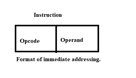
Example 1:
MVI A, 9AH
The operand is the part of instruction and stored in the register mentioned in the instruction.
Example 2:
ADI 05H
05H is the operand.
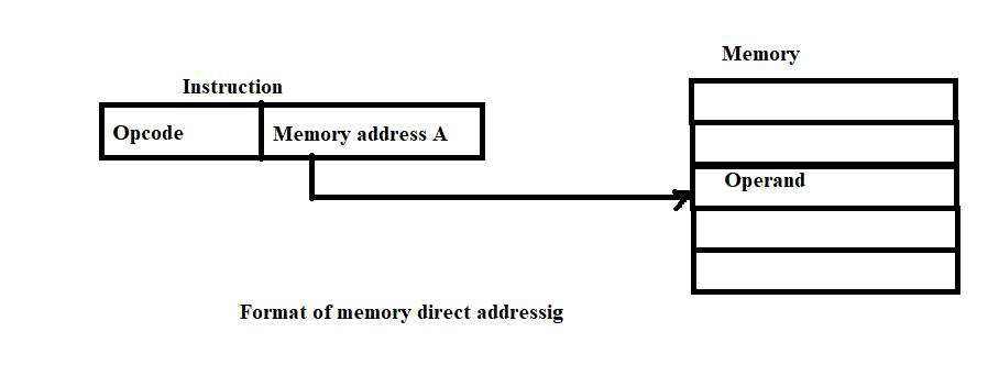
Memory direct addressing:
Memory direct addressing moves a byte between a memory location and register. It is also needed for data transfer between processor and input/output device.
Example 1:
LDA 850FH
Here the content of memory location 850FH is loaded to the accumulator.
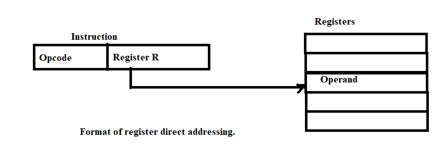
Register direct addressing:
Here data is copied from one source register to destination register.
Example 1:
MOV B, C
It copies the content of register C to register B.
Example 2:
Add C
It adds the content of register C to the accumulator and saves it to the accumulator.
Indirect addressing:
In this addressing mode the data is transferred from one register to another by using the third address that is the address pointed by the register. In other words it transfers the data from register to memory location and address of memory location is stored in the register and that register is specified in the instruction.
Example 1:
MOV A, B
Here the data is in the memory location and pointed by the contents of the HL pair and the data is moved to the accumulator.
Implied or implicit addressing:
Here the data which has to be operated is specified by the instruction itself.
For example CMA complements the contents of the accumulator.
Interrupts in 8085
Interrupt is the signal generated by another sources either internal or external to the CPU. While this signal is generated CPU transfers the control from its current program execution to another program of more importance or higher priority.
Interrupts are classified on the basis of their maskability, interrupt vector address and source.
Vectored and non-vectored interrupts:
In non-vectored interrupt the interrupt address is not known to the processor. They are useful for small systems because in small systems there are very few interrupt sources and the software structure is not complicated.
For example: INTR.
Vectored interrupts require the interrupt vector address to be supplied by the external device that gives the interrupt signal. This technique is also called as vectoring and it can be implemented in a number of ways.
For example: RST7.5, RST6.5, RST5.5, and TRAP.
Maskable and Non-maskable interrupts:
Maskable interrupts can be blocked and it can be done by software or hardware means.
For example: RST7.5, RST6.5, and RST5.5.
Non maskable interrupts cannot be blocked by writing some instruction into the program.
For example: TRAP.
Software and hardware interrupts:
Software interrupts transfer the control to a predefined ISR after execution.
For example: RST0, RST1, RST2, RST3, RST4, RST5, RST6, and RST7.
Hardware interrupts are signals given to the processor and there are 5 hardware interrupt pins in 8085.
For example: TRAP, RST7.5, RST6.5, RST5.5
8085 Instruction sets
An instruction is a bit pattern that is decoded inside a microprocessor to perform a specific function and the entire group of instructions that a microprocessor can decode is called its instruction set.
Intel 8085 processor has its own set of instructions listed both in in mnemonics and machine code.
Microprocessor 8085 instructions can be classified based on functionality, length and operand addressing. On the basis of functionality instructions are classified as:
Data transfer operations
Data transfer operations transfer data from one location of register to another location called destination register.
Arithmetic operations
Arithmetic operations include addition subtraction increment and decrement.
Logical operations
Logical instructions are accumulator oriented and they include AND, OR and EXOR.
Branching operations
Branching instructions transfer control of execution from one memory location to another either conditionally or unconditionally.
Machine control operations
Machine control operations control the execution of other instructions for example halting.
Rp : Register pairs.
Data transfer instructions:
| Mnemonics |
Functions |
| MVI |
Moves the 8-bit data. |
| LXI Rp, 16 bit |
Loads the 16-bit data in the register pair. |
| MOV |
Copies the data from the source to the destination. |
| LDA |
16-bit Loads the accumulator with the data from the memory location indicated by the 16-bit address |
| LHLD |
16-bit Loads the H and L registers directly from the two consecutive memory locations indicated by the 16-bit address |
| STA 16-bit |
Stores the contents of the accumulator in the memory location indicated by the 16-bit address. |
| SHLD 16-bit |
Stores the contents of the H and L registers in two consecutive memory locations indicated by the 16-bit address |
| PUSH Rp |
Pushes the contents of the register pair onto a stack |
| POP Rp |
Pops the top two memory locations of the stack onto a register pair. |
| OUT 8-bit |
Outputs the data in the accumulator to the port indicated by the 8 bit address. |
| IN 8-bit |
Inputs the data from the port indicated by the 8 bit address to the accumulator. |
| LDAX Rp |
Load accumulator with the contents of the memory location pointed to by the register pair. |
| STAX Rp |
Stores the contents of the accumulator in the memory location pointed to by the register pair. |
| XCHG |
Exchange the contents of the HL register pair with that of the D and E register pair. |
| SPHL |
Copy the contents of the H and L registers to the stack pointer. |
| XTHL |
Exchanges the contents of the HL register pair with the top of stack. |
Arithmetic Instructions:
| Mnemonics |
Functions |
| ADI |
Adds the 8 bit data to the contents of the accumulator. |
| ACI |
Adds the 8 bit data and the carry flag to the contents of the accumulator. |
| SUI |
Subtract the 8 bit data from the contents of the accumulator. |
| SBI |
Subtract the 8 bit data and borrow from the contents of the accumulator. |
| ADD |
Add the contents to the contents of the accumulator. |
| ADC |
Adds the contents and the carry to the contents of the accumulator. |
| SUB |
Subtract the contents from that of the accumulator. |
| SBB |
Subtract the contents and the borrow from that of the accumulator. |
| DAD |
Rp Add the contents of the register pair to that of the H and L registers. |
| INR |
Increments by 1 |
| INX Rp |
Increments the register pair by 1. |
| DCR |
Decrements t by 1 |
| DCX |
Decrements the register pair by 1. |
| DAA |
Converts the contents of the accumulator from binary to BCD. |
Logical Instructions:
| Mnemonics |
Functions |
| ANI 8-bit |
The 8 bit data is logically ANDed with the contents of the accumulator. |
| XRI 8-bit |
The 8 bit data is logically EXORed with the contents of the accumulator. |
| ORI 8-bit |
The 8 bit data is logically ORed with the contents of the accumulator. |
| ANA |
The contents are logically ANDed with the contents of the accumulator. |
| XRA |
The contents are logically EXORed with the contents of the accumulator. |
| ORA |
The contents are logically ORed with the contents of the accumulator. |
| RLC |
Rotate the bits of the accumulator left by one position. |
| RRC |
Rotates the bits of the accumulator right by one position. |
| RAL |
Rotates the bits of the accumulator left by one position, through the carry. |
| RAR |
Rotates the bits of the accumulator right by one position, through the carry. |
| CPI 8-bit |
Compares the 8 bit data with the contents of the accumulator. |
| CMP |
Compare the contents with that of the accumulator. |
| CMA |
Complements the contents of the accumulator. |
| CMC |
Complements the carry. |
| STC |
Sets the carry. |
Questions:
1. Exchange the contents of memory locations 8000H and 8055H using direct addressing.
Solution:
LDA 8000H : Load the content in accumulator.
MOV C, A : Move the content of accumulator to register C.
LDA 8055H : Load the content of memory location 8055H in accumulator.
STA 8000H : Store the contents of the accumulator in memory address 8000H.
MOV A, C : Move the saved contents in register C back to the accumulator.
STA 8055H : Store the content of accumulator in 8055H.
HLT : Terminates the program.
2. Add two numbers present in memory locations 7000H and 7001H. Place the results in a memory location 7002H.
Solution:
LXI H, 7000H : Load the first address 7000H in the HL register pair
MOV A, M : Load the first operand in the accumulator.
INX H : Load the second address 7001H by incrementing the HL pair by 1.
ADD M : Add the content of 7001H to the accumulator.
INX H : Load the third address 7002H by incrementing the HL pair by 1.
MOV M, A : Store the result of addition in 7002H.
HLT : Terminate program execution.
3. Subtract the contents of memory location 7001H from that of memory location 7000H and store the result in 7002H.
Solution:
LXI H, 7000H : Load the first address 7000H in the HL register pair
MOV A, M : Load the first operand in the accumulator.
INX H : Load the second address 7001H by incrementing the HL pair by 1.
SUB M : Subtract the second operand from the first.
INX H : Load the third address 7002H by incrementing the HL pair by 1.
MOV M, A : Store the result of addition in 7002H.
HLT : Terminate program execution.